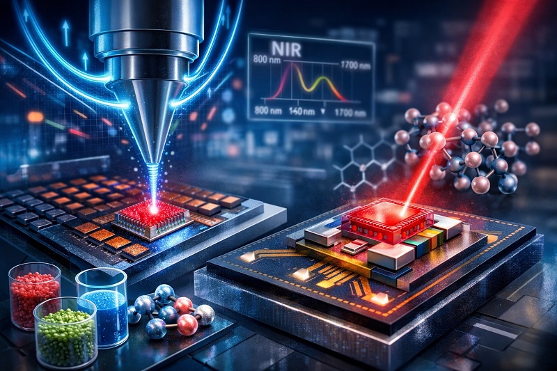
In recent years, electronics engineers have been trying to identify semiconducting materials that could substitute for silicon and enable the further...
Vous n'êtes pas connecté
- English
- Français
- عربي
- Español
- Deutsch
- Português
- русский язык
- Català
- Italiano
- Nederlands, Vlaams
- Norsk
- فارسی
- বাংলা
- اردو
- Azərbaycan dili
- Bahasa Indonesia
- Հայերեն
- Ελληνικά
- Bosanski jezik
- українська мова
- Íslenska
- Türkmen, Түркмен
- Türkçe
- Shqip
- Eesti keel
- magyar
- Қазақ тілі
- Kalaallisut ; kalaallit oqaasii
- Lietuvių kalba
- Latviešu valoda
- македонски јазик
- Монгол
- Bahasa Melayu ; بهاس ملايو
- ဗမာစာ
- Slovenščina
- тоҷикӣ ; toğikī ; تاجیکی
- ไทย
- O'zbek ; Ўзбек ; أۇزبېك
- Tiếng Việt
- ភាសាខ្មែរ
- རྫོང་ཁ
- Soomaaliga ; af Soomaali
Rubriques :
 Maroc - TECHXPLORE.COM - RSS news feed - 11/Jan 17:30
Ultra-small, high-performance electronics grown directly on 2D semiconductors
In recent years, electronics engineers have been trying to identify semiconducting materials that could substitute for silicon and enable the further advancement of electronic devices. Two-dimensional (2D) semiconductors, such as molybdenum disulfide (MoS₂), have proved to be among the most promising solutions, as their thinness and resistance to short-channel effects could yield highly performing and smaller electronics.
Articles similaires
Scientists print the world’s smallest infrared sensors—no silicon required
knowridge.com - 11/Jan 11:21
Engineers have created the smallest fully printed infrared light sensors ever made, opening a new path toward cheaper, smaller, and more flexible...
Scientists print the world’s smallest infrared sensors—no silicon required
knowridge.com - 11/Jan 11:21
Engineers have created the smallest fully printed infrared light sensors ever made, opening a new path toward cheaper, smaller, and more flexible...
Chinese scientists build 31.13%-efficient perovskite-silicon tandem solar cell via 2D seeding agent
pv-magazine-australia.com - 19/Jan 23:26
Researchers in China developed a novel two dimensional seeding agent to regulate crystallisation in a 1.80-eV wide-bandgap perovskite film. A...
Chinese scientists build 31.13%-efficient perovskite-silicon tandem solar cell via 2D seeding agent
pv-magazine-australia.com - 19/Jan 23:26
Researchers in China developed a novel two dimensional seeding agent to regulate crystallisation in a 1.80-eV wide-bandgap perovskite film. A...
100 million tons of CO2 by 2050: Electronic devices’ circuit boards drive largest carbon footprint
wn.com - 18/Jan 08:33
A new study has revealed that demand for healthcare electronics could approach 2 billion units per year by 2050. But unless measures are taken to...
100 million tons of CO2 by 2050: Electronic devices’ circuit boards drive largest carbon footprint
wn.com - 18/Jan 08:33
A new study has revealed that demand for healthcare electronics could approach 2 billion units per year by 2050. But unless measures are taken to...
Int'l research team develops damage-free etching technique for optoelectronic semiconductors
wn.com - 16/Jan 01:02
HEFEI, Jan. 15 (Xinhua) -- An international research team has developed a "self-etching" technique to process soft and unstable ionic crystal lattice...
Int'l research team develops damage-free etching technique for optoelectronic semiconductors
wn.com - 16/Jan 01:02
HEFEI, Jan. 15 (Xinhua) -- An international research team has developed a "self-etching" technique to process soft and unstable ionic crystal lattice...

Les derniers communiqués
-
Bank of America Reports Fourth Quarter 2025 Financial Results
Bank of America - 15/01/2026
-
GM Canada at the 2026 Montreal International Auto Show
General Motors - 15/01/2026
-
Cadillac Formula 1® Team Unveils Special Edition Livery for Barcelona Shakedown
General Motors - 13/01/2026
-
confidence with new 12-month/12,000 mile warranty
General Motors - 13/01/2026
-
organ Stanley Capital Partners Makes Majority Investment in Olsson, Inc.
Morgan stanley - 13/01/2026
-
Siemens named a leader in Green Quadrant: Quality Management Software 2025 report
SIEMENS - 12/01/2026
-
American rings in the new year with non-alcoholic IPA, new cocktails and refreshed menus in ight
AMERICAN AIRLINES - 12/01/2026
-
American Airlines partners with award-winning Pecan Lodge to serve Texas barbecue on select flights from DFW to New York airports
AMERICAN AIRLINES - 09/01/2026
-
American Airlines and OBAP celebrate 50 years of progress and 100 years of flight
AMERICAN AIRLINES - 07/01/2026
-
Lenovo unveils Qira AI assistant at CES 2026
Lenovo DE - 07/01/2026